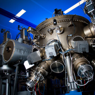
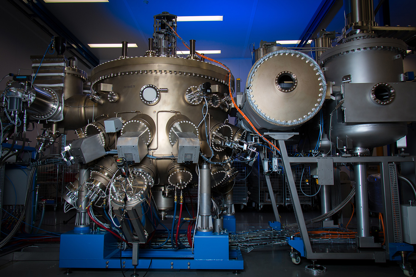
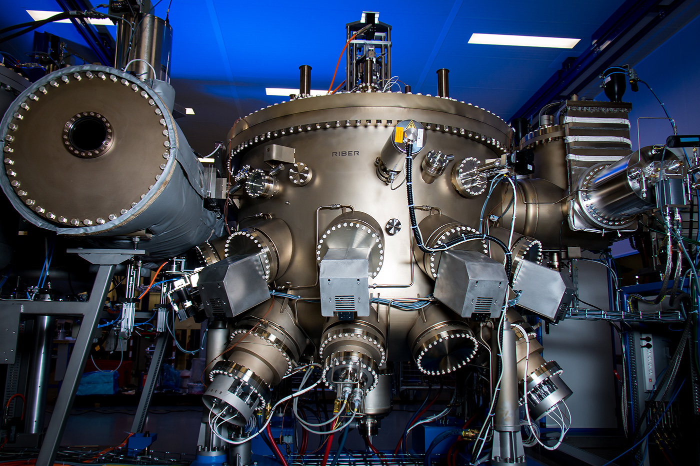
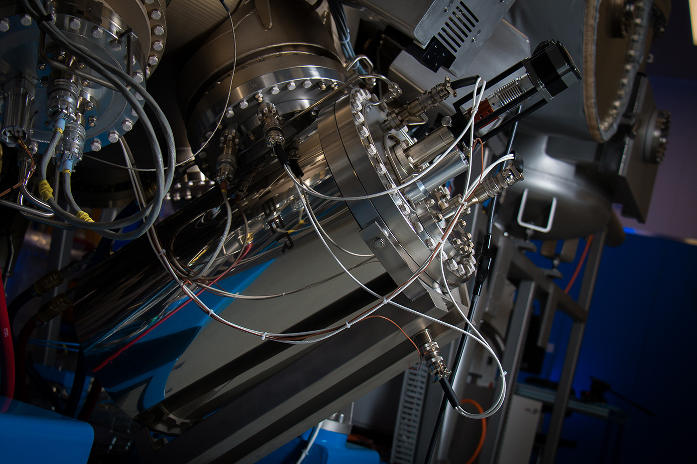
MBE 8000 – Production System
4×200 mm & 8×150 mm capabilities
Key features
- Twice the productivity of existing products
- Outstanding uniformities achievements
- High performance reproducibility run after run
Presentation
The system is designed to meet the growing needs of compound semiconductor devices with a high level of performance.
This 8×6ʺ or 4×8ʺ solid-source MBE system using ultra-pure metals in a UHV environment has exceeded fundamental state-of-the-art expectations in terms of design, temperature uniformity and flux uniformity for such a technology.
The system is capable of growing batches of eight 150 mm (6-inch) wafers or four 200 mm (8-inch) wafers with remarkable uniformities (composition, thickness) and very low levels of defects. The platform has been evaluated for the growth of 940 nm VCSELs (vertical cavity surface emitting lasers).
The experts’ final qualification in 2023 validated the MBE 8000 in terms of process, system robustness, stability, ergonomics and control.
Specifications
Guaranteed specifications over 8×6’’ platen
| Defect density | ≤ 50 /cm² |
| Thickness uniformity (InGaAs/GaAs)SL (DDX) | ± 1.5% |
| Composition uniformity (InGaAs/GaAs)SL (DDX) | ± 1.5% |
| Thickness uniformity (AlAs/GaAs)SL (DDX) | ± 1.5% |
| Si doping standard deviation uniformity | < 3% |
| FP-Dip uniformity of resonator | 3 nm |
| Background carrier density | 7×1014cm-3 |
| HEMT Electron mobility | 6000 cm²V-1s-1@RT 120 000 cm²V-1s-1@77K |
Best achievements
Thickness uniformity InGaAs/GaAs over 8×6’’ platen


