Applications & Markets
More than products, RIBER provides solutions, that enable research institutes as well as industrials to imagine and manufacture components of the future in various fields.
Power & RF Electronics
Transistors and amplifiers, III-V on Si, datacommunications, 5G and IoT, defense
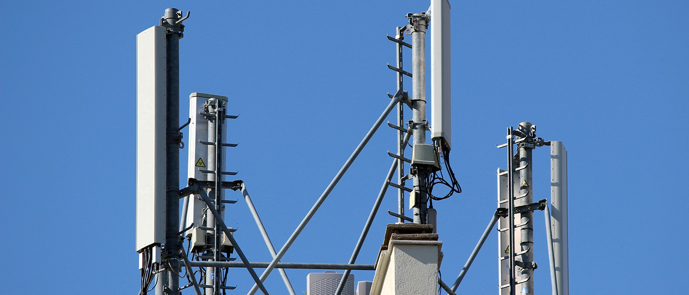
From the early 20th century, power electronics emerged as a main discipline in electrical engineering and as the basic technology for electric power conversion and control. The fields of application are broad, from industrial applications to transportation, renewable energy or defense applications.
GaN is typically a material used initially for defense power electronics – pulse RF power (radar), that found growing applications in civil uses. GaN is now driving the market growth of power devices, with its high breakdown voltage and high working frequencies.
For 5G communications, GaAs/GaN-based devices are seriously considered, to be used in RF transceivers of mobiles; GaAs and GaN are also candidates of choice in 5G antennas, where silicon devices cannot reach the required performance without increasing the number of channels, i.e., the number of antennas and corresponding electrical consumption, both in sub-6 GHz and 28-39 GHz ranges.
As a proof of technological maturity, constant efforts are put in integrating these III-V technologies onto Si substrate in order to benefit from the existing equipment in silicon foundries.
RIBER has significantly expanded its range of solutions in these fields, with increasingly innovative and high-performance.
Lasers
Datacenters, 3D sensing, LIDARs & Smart vehicles, medical and cutting, quantum computing
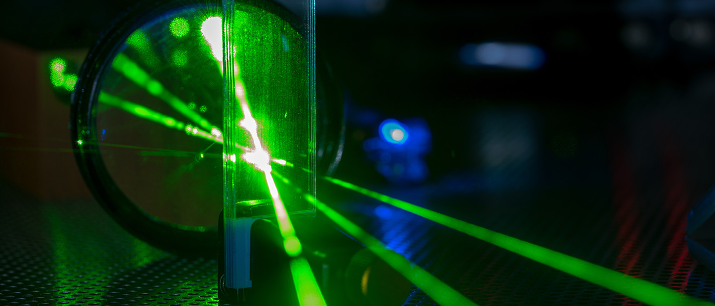
In the 60’s, invention of the Solid State Laser (SSL) initiated the surge of laser in everyday life. Nowadays, SSL is a key tool for modern technology, used in various applications such as laser cutting, welding, DNA sequencing, metrology or defense applications.
In the past years, QCLs pushed forward solid state laser solutions with high brightness and extreme spectral narrowness of the emitted light. Emitting in the mid to far IR spectrum, this type of semiconductor laser can be used in a variety of highly sensitive detectors.
From their initial use in short range & high speed data communications, VCSELs find new exciting applications for 3D sensing, eye tracking applications or LIDARs for smart vehicles.
Riber’s MBE solution brings these well-established technologies to unprecedented performance, enabling ultimate spectral narrowness and low defect density, reinforcing these devices’ specificity and reliability.
IR Detectors
Defense, Safety, LIDARs
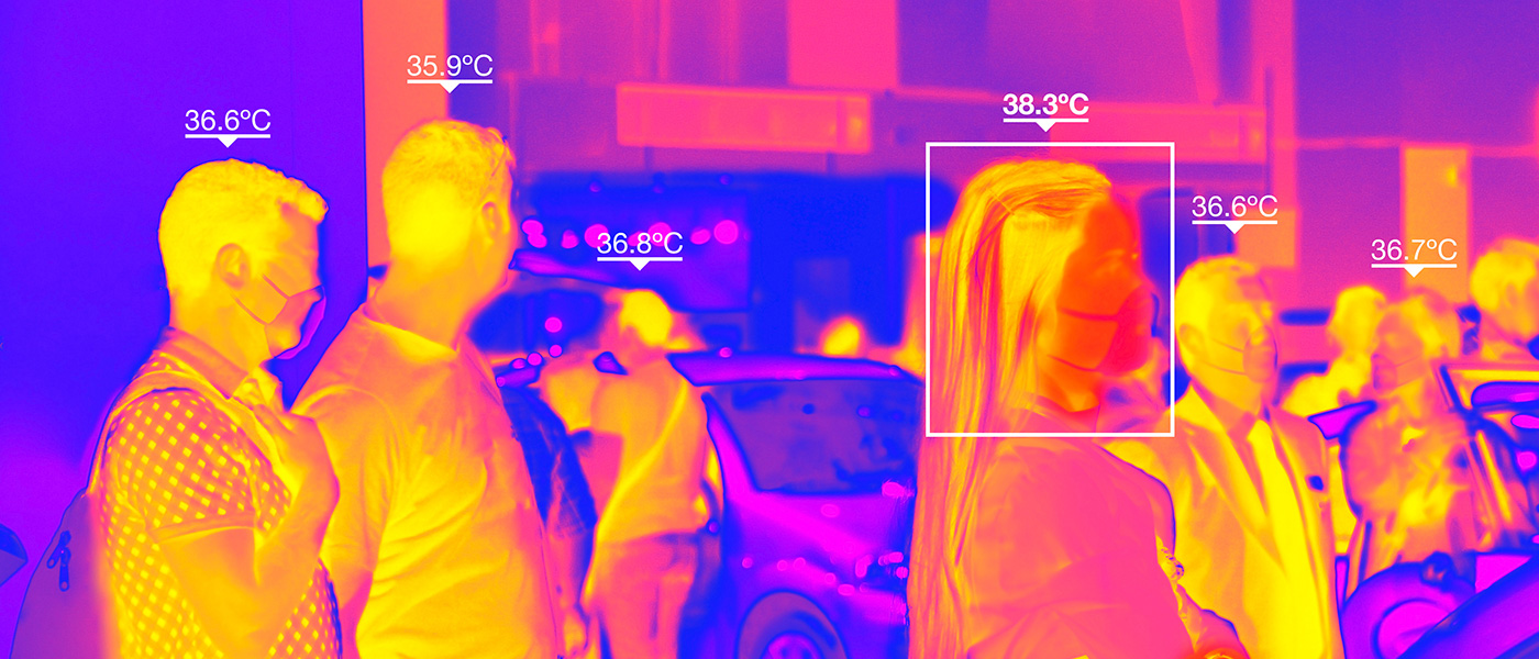
Well-established IR detectors are based on CdHgTe (Mercury Cadmium Telluride, MCT) technology. MCT is a semi-conductor alloy having the characteristic, amongst others, of interacting with infrared waves emitted by warm objects or living being. MCT infrared detectors, enables therefore to locate warm object in night environments: binoculars, photo cameras, cameras for night vision, surveillance or detection in both civil and military fields widely use this type of detector. Correct identification of the located object depends on the quality of the shape obtained by the detector, which must feature a very sharp analysis capability. Most infrared detectors providing such an acute quality are made from MBE epitaxial wafers, the only ones giving the necessary precision.
New generation of IR detectors, based on AlGaAs QWIPs or antimonides structures, emerged more recently. Usable for gas sensing, medical applications, automotive, consumer electronics or night detection, it covers the whole range of infrared spectrum, from SWIR (1-3 μm) to VLWIR (10-15 μm). Grown with classical III-V reactor design, it attracted strong interest: spatial uniformity and reproducibility are remarkable, they remain affordable and they work at normal temperature.
With a 20 year experience for this application in IR photodetectors (MCT and Sb-based), Riber’s technological advance in terms of design, manufacturing and start-up of this type of machine is recognized worldwide among the scientific and industrial community.
Displays
MicroLEDs, OLED
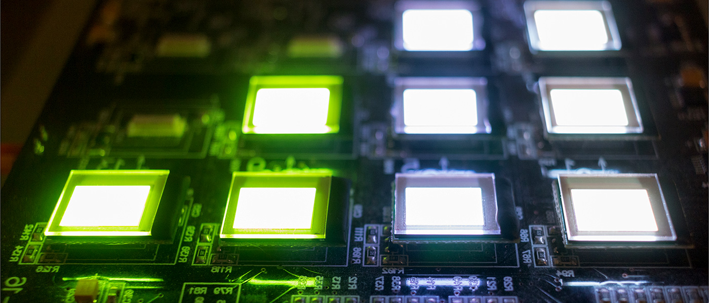
In the OLED technology, enabling electroluminescent flexible layers made of a thin film of organic compounds, challenges are now well established. Environmentally friendly, OLED display screens consume less power, offer wider angle visibility and deliver much brighter images than previous generations. First used for developing small screens (mobile phones, radios, notebooks, etc.), the OLED technology has gradually diversified with the manufacturing of flexible large screens and lighting (light sheets).
As a new disruptive technology, MicroLEDs is a booming field where MBE has a major role to play. These new components enable smaller pixels and higher brightness than existing display components; they introduce a real revolution in resolution compared to OLEDs. With its unique evaporation mode, MBE enables to incorporate easily high In fractions in GaN, enabling to cover the full visible spectrum without the need for phosphors or additional processing.
With its extensive portfolio of MBE equipment and innovative material evaporation solutions, Riber confirms its position as a major player for display manufacturing.
Passivation
Lasers, MicroLEDs, transistors and amplifiers
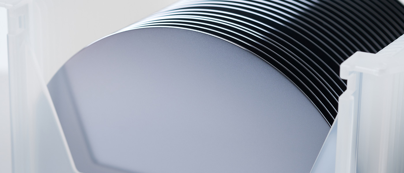
Passivation is a key step for several compounds semiconductor process. Inactivating the surface of the component enables to keep its properties safe and limit future defects generation, by avoiding unwanted oxidation, before further processing steps.
Initial Riber’s solutions have been developed for edge-emitting lasers, where Riber’s UHV solutions are used to passivate the laser facets and limit catastrophic optical damages (COD). Cleaning and passivation by ZnSe or SiN are available on Riber automated platforms.
Emerging materials
Topological insulators, 2D materials, functional oxides, superconductors, gallium oxide, quantum computing

Semiconductor research boundaries are far from being reached. Our customers constantly explores new areas to improve existing concepts or invent new approaches.
Whether it is for advanced information transport with high speed & ultra-low losses (topological insulators), very low thickness & heat management (2D materials), higher breakdown voltage (Ga2O3), improved reliability and mechanical resistance, easier integration in existing production lines and standards (integration of III-V materials on Si substrates), Riber experts are at customer’s side to shape the future of semiconductors.
Solar
III-V on Si, CIGS, perovskites

Silicon photovoltaics is no longer the only alternative on the solar energy market. Thin-film technologies, such as copper indium gallium (di)selenide (CIGS), III-V materials or perovskites structures have rapidly increased their market share. They promise a new era for photovoltaics, when the cost of energy produced by these thin-film cells is cost-competitive with traditional power generation.
One of the key steps in the manufacture of a thin-film cell is the deposition of a high-quality semiconductor layer. Riber has developed tools that excel in the area, enabling the deposition of CIGS layers that combine unprecedented material quality with exceptional uniformity of thickness and composition. Riber’s partnership with IPVF (https://ipvf.fr/) has led to remarkable results in the field of III-V cells on silicon in terms of cell yield.
RIBER’s first cell units were delivered to various partners since 2011 and have been incorporated into their pre-production processes.
OEM
Custom PVD thin films deposition
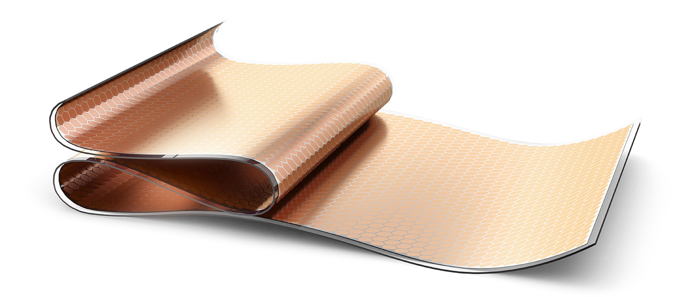
RIBER develops and markets evaporation sources for a wide range of applications covering OLED, Solar CIGS cells, batteries, anti-corrosion coating and plenty of advanced applications. RIBER is a key player in the manufacturing of PVD thin film deposition system and vacuum thermal evaporation technology for mass production.


