EZ-CURVE® Real-time curvature measurement
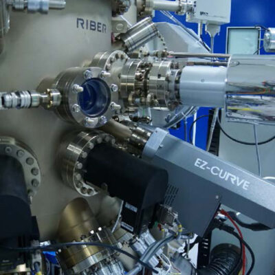
Monitor your thin film deposition and vacuum treatment process in real-time with Riber Magnification Inferred Curvature (MIC) tool
Main benefits
- In situ stress, bow and curvature measurement, in real time
- Set precise growth patterns and monitor deviations
- Detect specific growth events and retrieve fundamental knowledge about growth mechanisms
- Suitable for various thin films deposition techniques (CVD, MBE, PVD,…) and vacuum treatment process (plasma etching, annealing, quenching …)
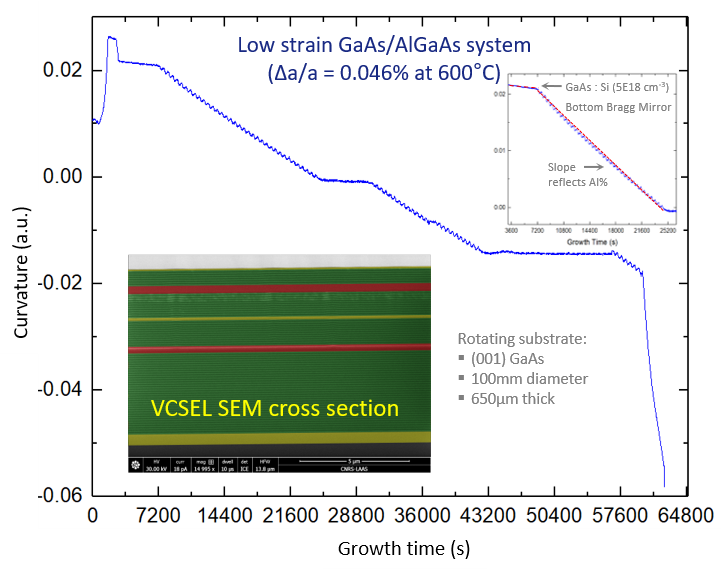
- Unrivalled curvature sensitivity
- Simultaneous spherical and cylindrical bowing, anisotropy measurement
- Compatible with low lattice mismatch systems like AlGaAs/GaAs
- Thick wafer compatible -up to few mm
- Highly stable & alignment-free measurement
- Wide-range wavelength source – immune to reflectivity change, no need to adjust exposure time
- Immunity to wafer flatness – possible use with patterned wafer
Key features
| Parameter | Specifications |
|---|---|
| Curvature range (min – max) | 0,0008 – 200 000 km-1 |
| Sensitivity (1-std dev) | Up to 8×10⁻⁷m-1 (5×5 matrix, 5s integration/ 500 points –θ= 70°) |
| Measured standard deviation | 8.33×10⁻⁶m-1(θ= 0°) // 2.85×10⁻⁶m-1(θ= 70°) |
| Radius range (max – min) | 1 250 000 -5×10⁻³m |
| Source lifetime | 50 000 h |
| Measurement frequency | 100 Hz |
| Rotation speed range | 0-100 rpm |
| Viewport to sample distance | Adjustable from 75 mm – depending on vacuum chamber dimensions |
| Flexible installation angle on the reactor | 0 – 70° |
For additional & detailed information, please visit:
Software
- Curvature, Stress, Phase and Anisotropy measurement & display
- Intuitive data acquisition
- Powerful data saving functions
- Real time mode up to 100 fps
- Flexibility to share data with other software incl. Riber Crystal XE
- Post-processing and data treatment
- Remote modbus interface
References
Find out more about EZ-CURVE here :
- Nature Scientific reports : Magnification inferred curvature for real-time curvature monitoring
- Journal of Applied Physics : Links between bismuth incorporation and surface reconstruction during GaAsBi growth probed by in situ measurements
- ACS Applied Energy Materials: Thickness Limitation of Band-to-Band Tunneling Process in GaAsSb/ InGaAs Type-II Tunnel Junctions Designed for Multi-Junction Solar Cells


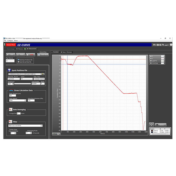 RIBER - EZ-CURVE® Software
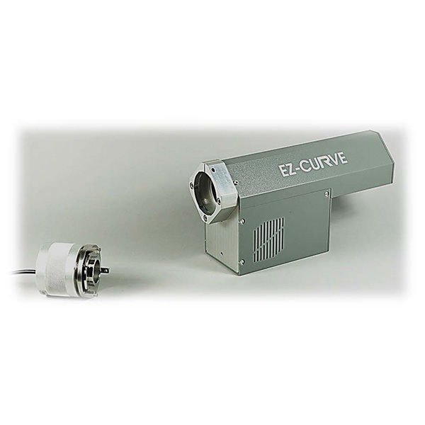 RIBER - EZ-CURVE®
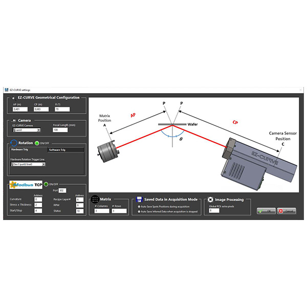 RIBER - EZ-CURVE® software


